
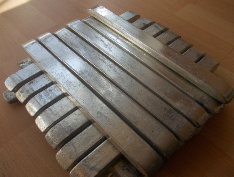

Description
Features:
1. High purity, good infiltration.
2. Clean, beautiful, after welding, insulation, high resistance, low ionic contamination, PCB board welding residual minimal.
3. Good oxidation resistance, low tin slag and cost savings.
4. Solder joint is bright, full and uniform.
5. Economical and can produce the lowest consumption of most of the solid solder joints.
Applications:
It is mainly used in the manufacture of compound semiconductor, High purity alloy, superconducting material, Solder and as a dopant of compound semiconductor.
Information is up-to-date: 07.03.2018
Read more
Unbelievable price on Tin ingots in Kuala Lumpur (Malaysia) company Rassvet, Sdn. Bhd..